Field of expertise:
Methods:
Application area:
Industry:
Aerospace and Defence| Consumer Products| Energy Sector| Semiconductor
Story
Our electronic devices are almost unimaginable without some kind of printed circuit board (PCB) and/or integrated power electronic module (IPEM). The increased use of these devices (e.g. automotive, industrial and consumer electronics) creates more opportunities today for electromagnetic compatibility (EMC) issues. EMC requires that electrical equipment be able to tolerate a specific degree of electromagnetic interference (EMI) and not generate more than a specified amount of interference. Also, with the increase in high-frequency content, the influence of previously negligible circuit parasitics starts to play an increasing role in EMI production [1].
The main reasons for manufacturers paying so much attention to EMI issues on their products [2]:
- a product will be prohibited to sell in the markets if it fails the EMI standards;
- to comply with EMI requirements by modifying the design, increase the cost and cause the product’s price to be non-competitive in the marketplace;
- additional schedule delays resulting from solving the EMI problem can make the product announcement miss the window of optimum marketability, inevitably, leading to reduced sales.
The numerical simulation helps to avoid or reduce the above-mentioned problems at an early stage of the design process.
Ansys electromagnetic software (Maxwell, HFSS, Q3D Extractor) can help the extraction of parasitic parameters, analysis of the operation and optimise the layout of the circuit in the concept or design stage.
The following example demonstrates the strength of Ansys tools to simulate a printed circuit board with an emphasis on impedance computation and compare results with measurement.
Simulation of PCB Structure
The analysed example is an FR-4 PCB board with a copper trace and ground as you can see in Fig. 1 and 2. This is an example from [2] where you can find a detailed description of the geometry, the materials and the impedance measurement.
Through this example, we demonstrate the capabilities of four software from Ansys EM portfolio (Maxwell, Q3D, HFSS and HFSS 3D Layout). These are all suitable for the analysis of parameters and parasitic phenomena of PCB or DBC (direct bonded copper) structure. The tested software is:
- Maxwell 3D / Maxwell 2D
Ansys Maxwell is a general finite element method based simulation software for the design and analysis of low-frequency electromagnetic devices (e.g. electrical motors, sensors). With Maxwell, you can precisely characterize the linear or nonlinear behaviour and parameters of electromagnetic components and their effects on the drive circuit and control system design [3].
The eddy current (frequency domain) solver of Maxwell used in this example. - Q3D Extractor / 2D Extractor:
Ansys Q3D Extractor efficiently performs the 3D and 2D quasi-static electromagnetic field simulations required for the extraction of RLGC parameters from an arbitrary electromagnetic structure. It then automatically generates an equivalent SPICE circuit model. These accurate models can be used to perform signal integrity analysis to study electromagnetic phenomena, such as crosstalk, ground bounce, interconnect delays and ringing, to understand the performance of interconnects, IC packages, connectors, PCB’s, bus bars and cables [4]. - HFSS (High Frequency Structure Simulator)
Ansys HFSS is a 3D electromagnetic simulation software for designing and simulating high-frequency electronic products such as antennas, antenna arrays, RF or microwave components, high-speed interconnects, IC packages and PCBs. Engineers worldwide use Ansys HFSS to design high-frequency, high-speed electronics found in communications systems, radar systems, advanced driver assistance systems (ADAS), internet-of-things (IoT) products and other high-speed RF and digital devices [5].
Ansys HFSS 3D Layout is a design type within the Ansys HFSS product. HFSS 3D Layout can be extensively used for simulations with layers, nets, components and padstacks. It also contains multiple solver types. HFSS 3D Layout structures geometry in terms of layers that are common in electronic computer-aided design (ECAD), including printed circuit board (PCB) layout, RF/microwave circuits or planar antennas and components.
There is no need to deal with discretization in all the solvers because the adaptive meshing reduces the local error at the right places to achieve the accurate result. The final adaptive mesh of simulations can be seen in Fig 3.
As we can see in this figure, the discretisation and the number of elements are different, because of the different numerical technique and solver in the background. However, this difference does not appear in the solution as we can see in Fig 4 and 5. Fig. 4 and 5 show the magnitude and phase of impedance for the example PCB structure between 1kHz and 1MHz frequency. The amplitude of the impedance is practically the same for all calculations and for the measurement. A similarly good match is observable in the case of the phase of impedance for all of the solvers.
In the second half of the examined frequency range, twice the penetration depth (skin depth) is comparable or smaller to than the size of the trace. In other words, the current displacement (skin effect) caused by the eddy current already appears in the simulation, as shown in Fig. 6. So, Fig. 4 also support, that the Ansys software accurately handles the effect of eddy current. It is also suitable for analysis over a wide frequency range. In this example, the frequency is limited to 1 MHz by the impedance analyzer.
Conclusions
The used example shows well that Ansys electromagnetic products provide an equally accurate solution. However, each software has been developed for a different frequency range or application. Maxwell is a general low-frequency simulation tool. HFSS and HFSS 3D Layout are general high-frequency simulation tool. Q3D is a special tool for extraction of RLGC parameters.
In the point of view of simulation resource, the two-dimensional solvers seem to be efficient. But the main reason for this is the simplicity of the example. For example, in the power module shown in Fig. 7, three-dimensional simulation is unavoidable.
It is important to mention that there are two more software in the Ansys portfolio. SIwave is specialized and well automated design platform for power and signal integrity and EMI analysis of IC packages and PCBs. EMC Plus specializes in analyzing lightning-induced electromagnetic (EM) effects on large platforms and cable EMI/EMC problems in aircraft and automobile platforms to support EMC certification.
References
[1] X. Gong, J. A. Ferreira: „Comparison and Reduction of Conducted EMI in SiC JFET and Si IGBT-Based Motor Drives”, IEEE Transactions on Power Electronics, Vol. 29, No. 4, 2014, pp. 1757-1767. [2] J. Qian: “RF Models for Active IPEMs”, Master Thesis, Virginia Polytechnic Institute and State University, 2003. [3] Ansys Maxwell – https://www.ansys.com/products/electronics/ansys-maxwell [4] Ansys Q3D Extractor – https://www.ansys.com/products/electronics/ansys-q3d-extractor [5] Ansys HFSS – https://www.ansys.com/products/electronics/ansys-hfss
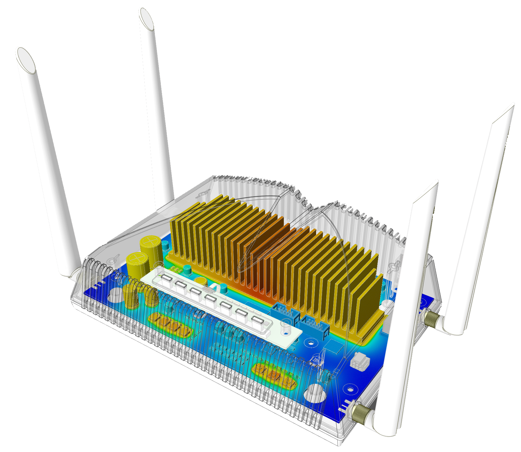
Fig. 1) The electric field strength on the surface of PCB in Q3D Extractor
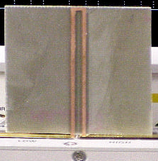
Fig. 2) The arrangement of impedance measurement [2]
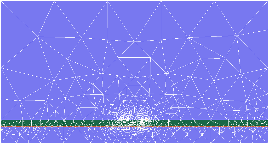
a) Maxwell 2D – 1 798 elements [3]
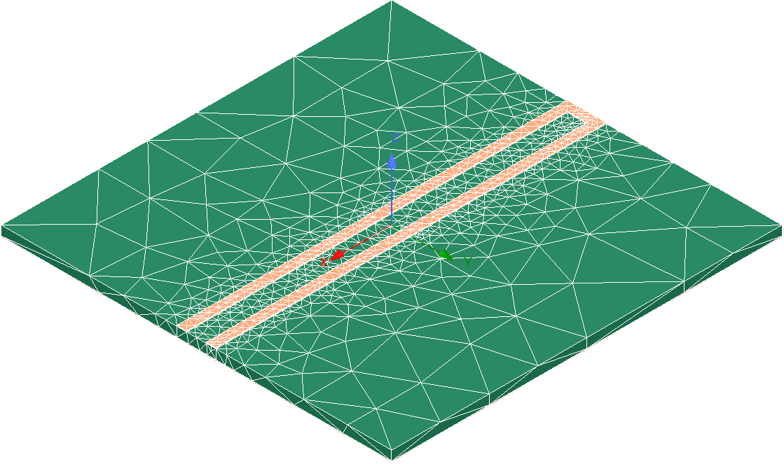
b) Maxwell 3D – 26 600 elements [3]
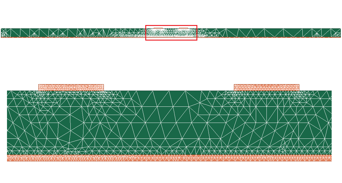
c) 2D Extractor – 3 637 elements [4]
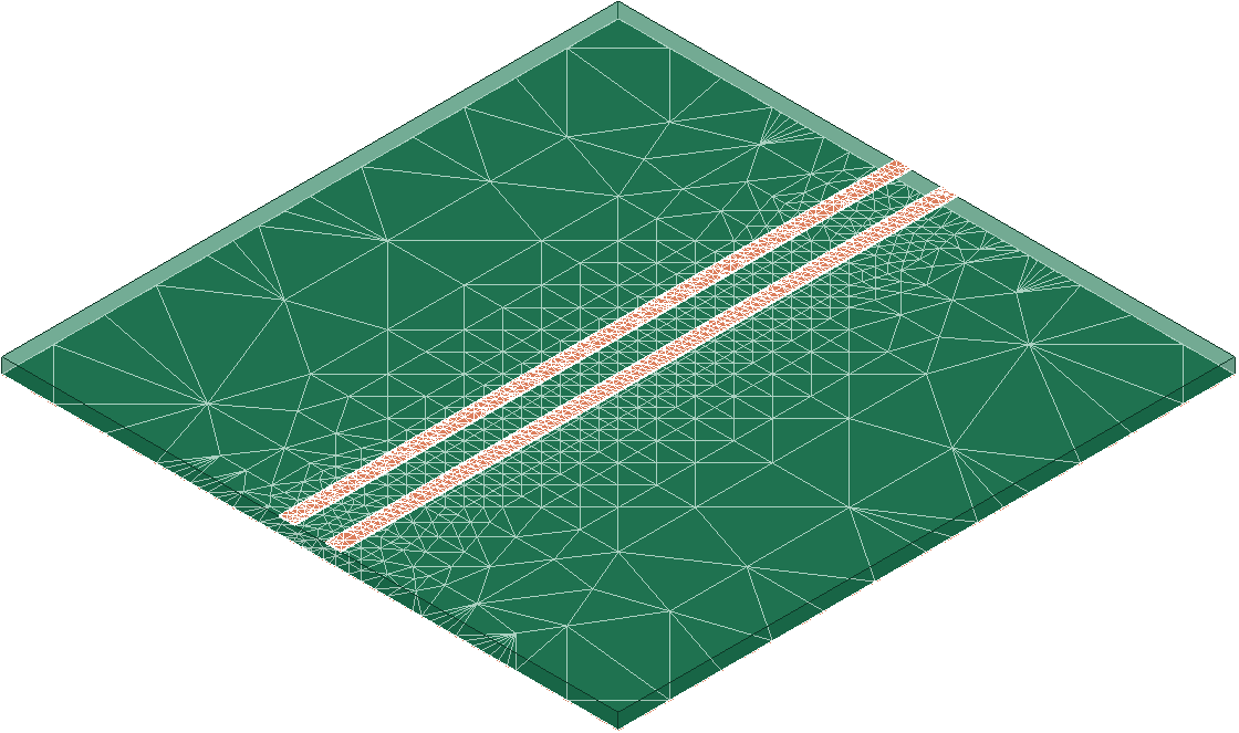
d) Q3D Extractor – 10 614 elements [4]
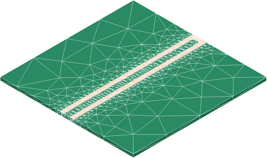
e) HFSS – 29 574 elements [5]
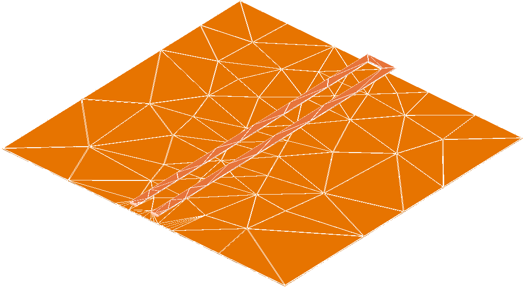
f) HFSS 3D Layout – 4 474 elements [5]
Fig. 3) The final discretization of the problems is at the end of the adaptive meshing process.
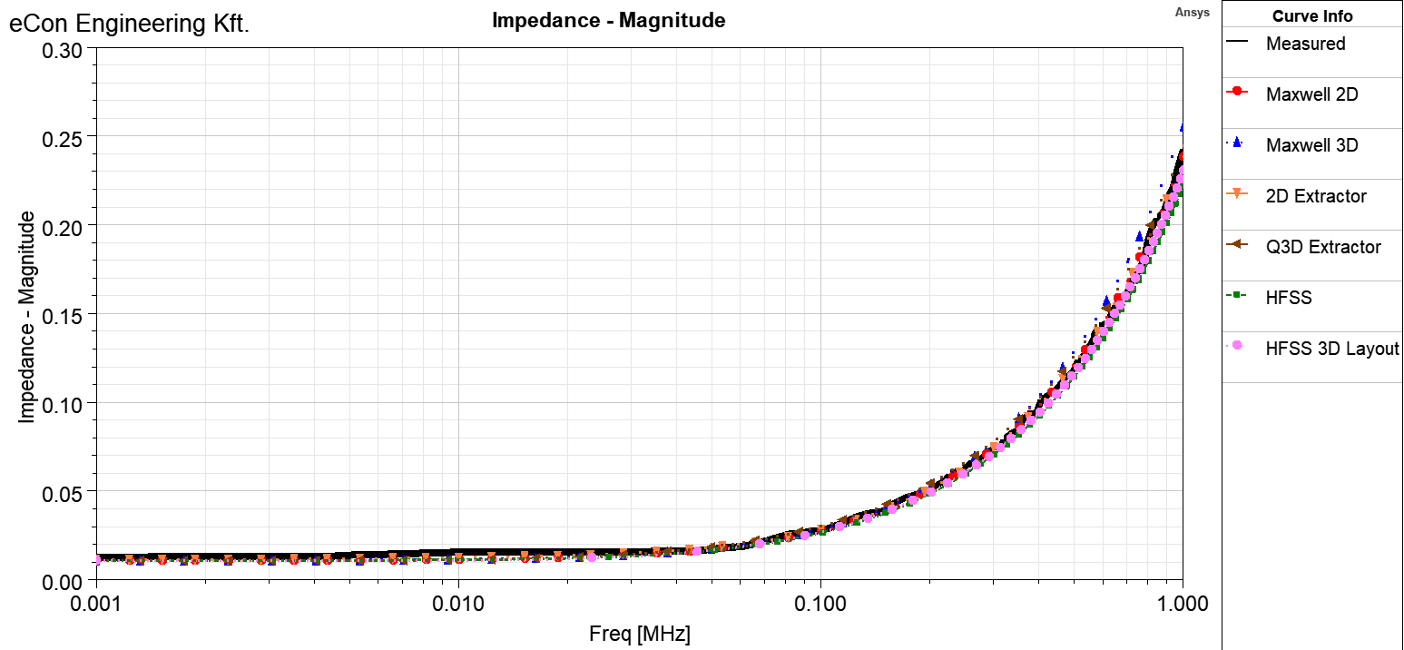
Fig. 4) The magnitude of calculated and measured [2] impedance for PCB structure.
![PCB Structure Fig5_ImpedancePhase The phase of calculated and measured [2] impedance for PCB structure.](https://econengineering.com/wp-content/uploads/2024/06/Fig5_ImpedancePhase.png)
Fig. 5) The phase of calculated and measured [2] impedance for PCB structure.
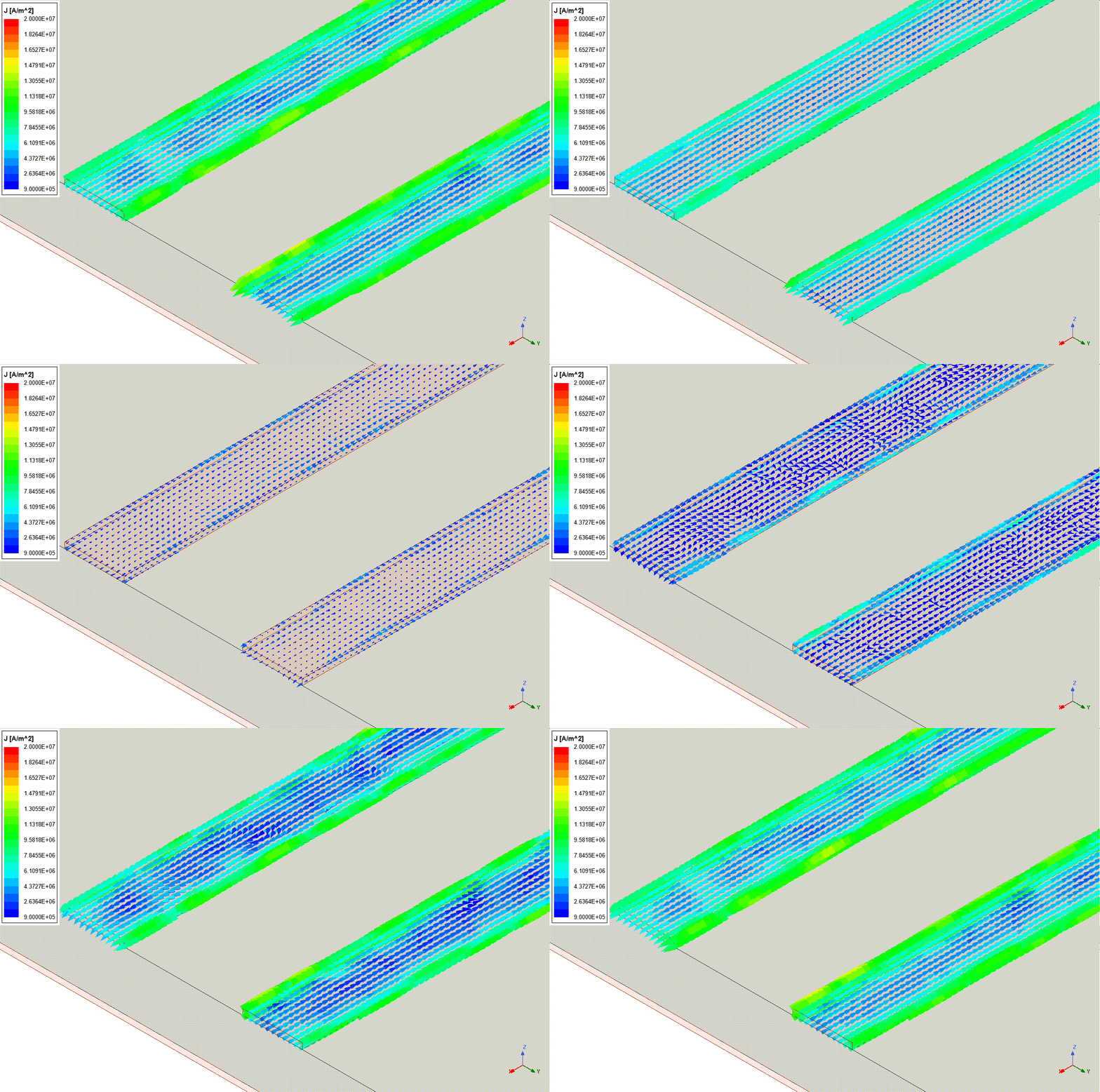
Fig. 6) The vectors of current density in the copper trace at 1MHz (Maxwell 3D).
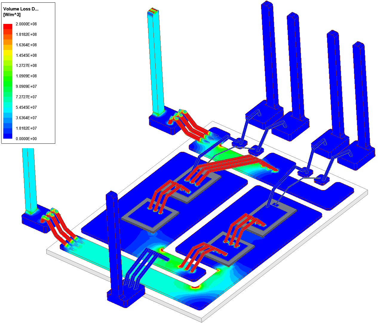
Fig. 7) EM loss of power module in Q3D Extractor.
